Semiconductors are the brains of our digital world. Their processing power enables us to have advanced medical equipment, smartphones, computers, space travel, and more. Since they are the basis of so much technology, their advancement is key to innovation.
While semiconductor chips themselves are impressive, the impeccable precision required to make them is even moreso. These multi-billion dollar fabrication plants, also known as fabs, contribute to a massive global industry, with revenues that are projected to surpass $1 trillion by 2025.
To meet design and manufacturing demands, fabs must ensure that they are protected from seismic activity with appropriate seismic bracing measures.
About Semiconductor Chips

Without semiconductor chips, many of the world’s life-changing advances would not be possible. The modern semiconductor chip enables smartphones to have more combined processing power than the computers that landed man on the moon in the 1960s.
According to the Semiconductor Industry Association (SIA), a single semiconductor chip has as many transistors as all of the stones in the Great Pyramid in Giza. With over 100 billion integrated circuits in use globally, this is equivalent to the number of stars in our part of the Milky Way galaxy.
These chips have allowed for breakthroughs in communication, transportation, clean energy, healthcare, and more. They continue to pave the path for innovation, running not only the modern world, but mapping out the future one.
As such, the semiconductor industry is booming – and to meet demand, more fabrication plants are being built. The United States is a hot spot for fab construction.
What Goes Into A Semiconductor Fabrication Plant
Also known as a fab or a foundry, these factories require many expensive devices in order to function. As demands for more advanced chips grow, so too do the expenses of both building and maintaining the environment necessary to fabricate them. These skyrocketing costs mean that new fabs can cost billions of dollars.
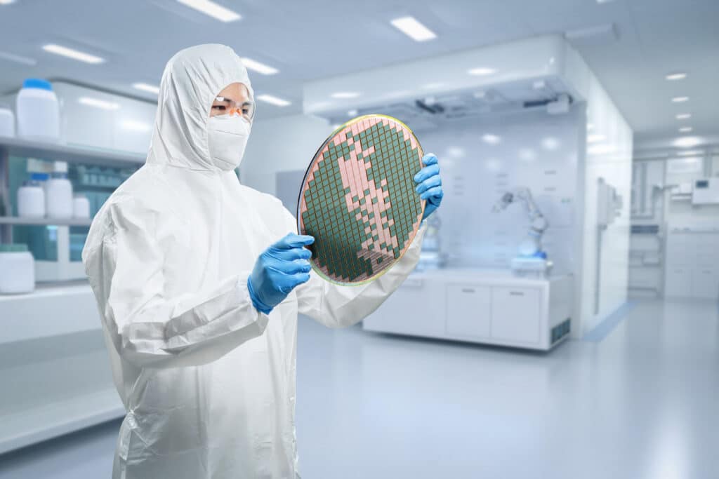
The central part of a fab is the clean room, where all fabrication takes place and where all the machinery for circuit production is. The environment is controlled to eliminate all dust, as even a singular speck could ruin a microcircuit. It must also be damped against vibration in order to ensure nanometer-scale alignment of machines, as well as being kept within a very specific band of temperature and humidity so as to minimize static electricity.
Fabs also have air handling equipment, an air plenum, a return air plenum, the clean subfab with support equipment, the ground floor, and office space. The equipment used for fabrication ranges from $700,000 to hundreds of millions of dollars each, with typical semiconductor fabrication plans having hundreds of equipment items.
Seismic Engineering: Protecting Our World To Build Our Future
Semiconductors are one of the top five American exports, and the semiconductor industry employs over 250,000 people in the United States while supporting approximately 1.8 million additional U.S. jobs. Seismic bracing is necessary to protect specialty systems, equipment, and the life-safety of fabs.
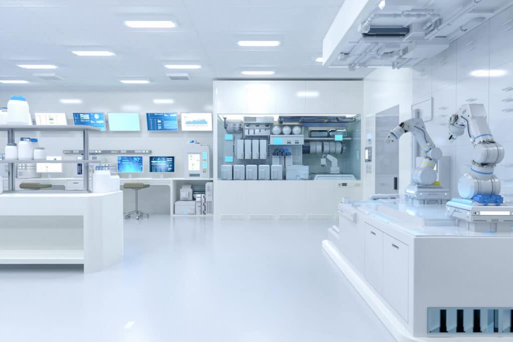
While semiconductor fabrication plants themselves are generally designed to either meet or exceed code requirements, the vibration-sensitive equipment is often left exposed to the lateral loads of seismic events. Seismic bracing, equipment anchorage, and equipment seismic certification are all ways fabs can protect their systems. This prevents otherwise disastrous damage that doesn’t just render fabs non-functional, but also result in devastating economic consequences.
Nearly everything in a fab needs some kind of seismic anchorage and bracing. Non-structural systems in general tend to be more valuable than the structure, and this is especially true when it comes to fabs. These very specialized systems are far, far more valuable than the structure. As such, obtaining secure seismic bracing is essential. Fabs run continuously and seismic bracing enables them to continue functionality during and after a seismic event.
All-Inclusive Seismic Bracing Solutions For Fabs
VIE is qualified to provide seismic engineering services for all types of facilities, high-tech facilities like computer chip manufacturers included. Our seismic bracing solutions go beyond meeting code requirements with project-specific designs that improve the safety of structures while reducing seismic damage and downtime following a seismic event.
Our equipment anchorage designs prevent fab equipment from being knocked off of supporting structures and minimize long-term costs through preventing non-structural systems from moving during a seismic event.
In addition to our seismic bracing and anchorage designs, we are one of the few engineering firms in the United States that provides equipment seismic certification through analysis methods rather than shake-table testing. This use of experience data is approved by multiple review authorities, such as the IBC and ASCE-7, and saves our clients hundreds of thousands of dollars.
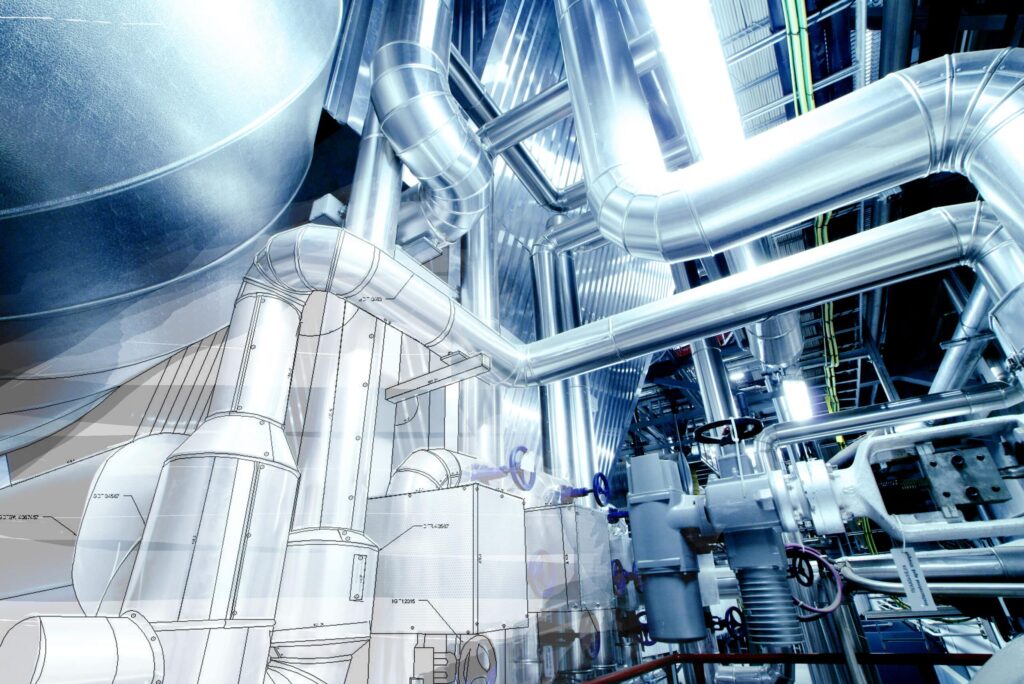
Furthermore, VIE was invited to speak at the Fifth International Workshop on the Seismic Performance of Non-Structural Elements (SPONSE). VIE spoke about practical considerations for non-structural bracing design of multiple suspended utilities in congested areas of facilities, relevant to fabs.
With a total construction value approaching $10 billion in the past 7 years alone, VIE enables our clients to prepare for the future through mitigating risk and preserving the safety of people and property alike. Contact us for more information about our seismic engineering services, the previous projects we have completed, or to request a consultation.

